Today the company will make a fuss with the first devices that have a new type of chip
With the new processor, users of these devices can edit 4K video, modify high-resolution photos, and play graphically intensive games more easily than previously possible using fewer battery.
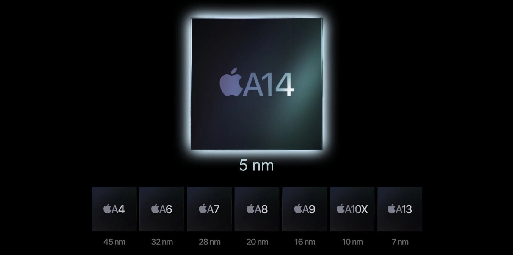
The new 5-nanometer architecture means that the size of the transistors has been reduced and the processor board occupies more of them than was previously possible. These transistors are now only 25 atoms wide and billions of them can be placed on a single plate. Simply put, more processing power. Four years ago the industry doubted that such an advancement would be possible.
Such advancements would not have been possible before an unknown Dutch company called ASML. This company has developed a way to construct transistors on the silicon plate through a process called Extreme Ultraviolet (EUV). Its machinery costs $123 million a share. It is currently the only company that manufactures these devices and they are more cost-effective than alternative options due to the low level of defects.
Only two chipmakers have started using this technology commercially:
- Taiwan Semiconductor Manufacturing Company (TSMC) – the only supplier with Apple A14 processor for iPhone, iPad, and Mac
- Samsung – which is producing the new Qualcomm processor that will debut in December
Both firms have their share in ASML alongside Intel which will start using the technology in 2021.
What exactly does 5-nanometer mean?
One nanometer is one of 1 billion Metter. This is the size that human hair grows every second. Transistors are used to measure the width of a component. But a decade ago the way chips are designed changed and nanometers are no longer used as a geometric effect. Today 5 nanometers is more of a marketing term and two companies with the same design can produce transistors with different performance.
To help you understand the size of transistors, at every 1 mm2 of the Apple chip are put 17,1 million transistors. The new structure with a stack of four nanosheets allows about 30 transistors to be placed onto the chip with the size of a fingernail bringing significant gains in efficiency and power.
In comparison to the 10 nm chip, the new 5 nm structure brings 40% performance improvements at fixed power, or 75% power saving at matched performance. This leads to more powerful and more efficient smaller devices.
N5 is the first TSMC process designed around extreme ultraviolet lithography (EUV). Because it uses a 13.5-nanometer light instead of 193-nanometers, EUV can define chip features in one step—compared with three or more steps using 193-nanometer light.
> Check next: iPhone 12 Last Minute Rumors: Better Zoom and Longer Battery Life
So what do you think about this? Let us know your thoughts in the comments section below, follow us on Twitter and Facebook for more news and updates.